Next-generation Computing Materials
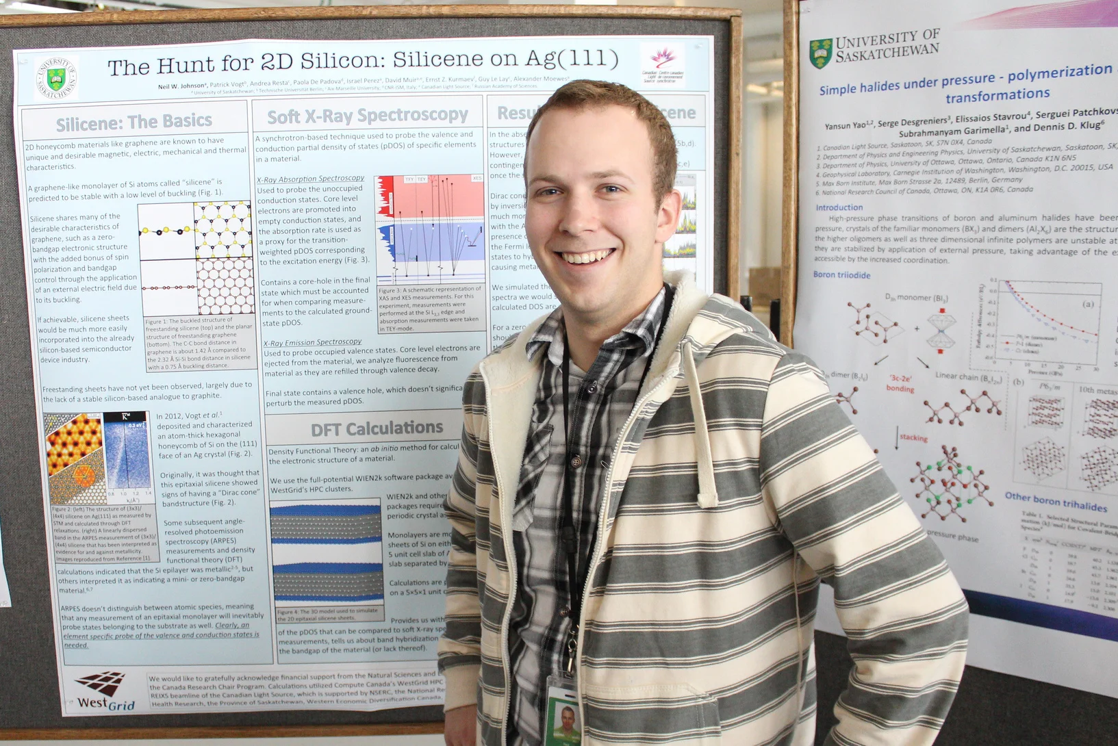
As computer chips continue to get smaller and more powerful, the field of electronics is approaching some severe limits. “Once a device becomes too small it falls prey to the strange laws of the quantum world,” says University of Saskatchewan researcher Neil Johnson, who is using the Canadian Light Source synchrotron to help develop the next generation of computer materials. Johnson is a member of Canada Research Chair Alexander Moewes’ group of graduate students studying the nature of materials using synchrotron radiation.
His work focuses on silicene, a recent and exciting addition to the class of two-dimensional materials. Silicene is made up of an almost flat hexagonal pattern of silicon atoms. Every second atom in each hexagonal ring is slightly lifted, resulting in a buckled sheet that looks the same from the top or the bottom.
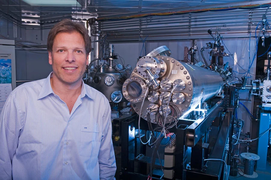
In 2012, mere months before Johnson began to study silicene, it was discovered and first created by the research group of Prof. Guy Le Lay of Aix-Marseille University, using silver as a base for the thin film. The Le Lay group is the world-leader in silicene growth, and taught Johnson and his colleagues how to make it at the CLS themselves.
“I read the paper when the Le Lay announced they had made silicene, and within three or four months, Alex had arranged for us to travel down to the Advanced Light Source with these people who had made it for the first time,” says Johnson. It was an exciting collaboration for the young physicist.
“This paper had already been cited over a hundred times in a matter of months. It was a major paper, and we were going to measure this new material that no one had really started doing experiments on yet.”
The most pressing question facing silicene research was its potential as a semiconductor. Today, most electronics use silicon as a switch, and researchers looking for new materials to manage quantum effects in computing could easily use the 2-D version if it was also semiconducting.
Calculations had shown that because of the special buckling of silicene, it would have what’s called a Dirac cone - a special electronic structure that could allow researchers to tune the band gap, or the energy space between electron levels. The band gap is what makes a semiconductor: if the space is too small, the material is simply a conductor. Too large, and there is no conduction at all.
Since silicene has only ever been made on a silver base, the materials community also wondered if silicene would maintain its semiconducting properties in this condition. Though its atomic structure is slightly different than freestanding silicene, it was still predicted to have a band gap. However, silver is a metal, which may make the silicene act as a metal as well.
No one really knew how silicene would behave on its silver base.
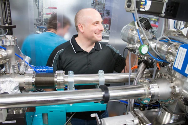
To adapt the Le Lay group’s silicene-growing process to the equipment at the CLS took several days of work. Though their team had succeeded in silicene synthesis at the Advanced Light Source at Berkeley lab, they had no way to keep those samples under vacuum to prevent them from oxygen damage. Thanks to the work of fellow beamteam members Drs. David Muir and Israel Perez, samples grown at the CLS could be produced, transported and measured in a matter of hours without ever leaving a vacuum chamber.
Johnson grew the silicene sheets at the Resonant Elastic and Inelastic X-ray Scattering (REIXS), beamline, then transferred them in a vacuum to the XAS/XES endstation for analysis. Finally, Johnson could find the answer to the silicene question.
“I didn’t really know what to expect until I saw the XAS and XES on the same energy scale, and I thought to myself, that looks like a metal,” says Johnson.
And while that result is unfortunate for those searching for a new computing wonder material, it does provide some vital information to that search.
“Our result does help to guide the hunt for 2-D silicon in the future, suggesting that metallic substrates should be avoided at all costs,” Johnson explains. “We’re hopeful that we can grow a similar structure on other substrates, ideally ones that leave the semiconducting nature of silicene intact.”
That work is already in process, with Johnson and his colleagues planning to explore three other growing bases this summer, along with multilayers and nanoribbons of silicene.
The paper this article discusses is: Johnson, N. W., Vogt, P., Resta, A., De Padova, P., Perez, I., Muir, D., Kurmaev, E. Z., Le Lay, G. and Moewes, A. (2014), The Metallic Nature of Epitaxial Silicene Monolayers on Ag(111). Adv. Funct. Mater., 24: 5253-5259. doi: 10.1002/adfm.201400769
$nbsp;
